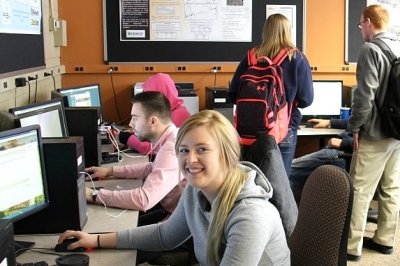
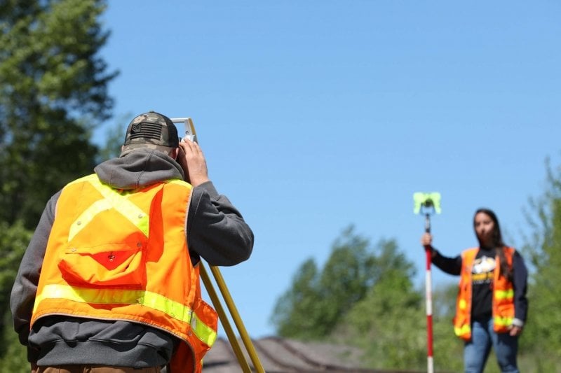
| |
Abstract |
Thin films of many different materials on the same substrate are required for advanced semiconductor, optoelectronics and microelectromechanical (MEMS) devices. However, in most cases, it is not possible to grow different materials with desirable properties such as crystallinity, microstructure, and electrical or optical functionalities, on the same substrate because of lattice mismatch, interdiffusion, and reaction with the substrate material. In particular, it has been difficult to grow good quality metal-oxide films on semiconductors for on-chip integration of semiconductor lasers with thin film optical isolators and modulators, both based on metal-oxides. Thus, the development of a technique to manipulate thin films of different materials, particularly metal-oxide ferroelectrics, is crucial for many engineering applications.
The research proposed seeks to provide a reliable process for the separation of ferroelectric films and attaching onto a dissimilar substrate. It is anticipated that optimum conditions for separation of films of a number of technologically important ferroelectric materials will be generated. This will result in a successful implementation of the process for manufacturing of microsystems comprised of ferroelectric films. The mechanism responsible for the layer separation process will also be clearly understood through the use of extensive use of transmission electron microscopy (TEM), thus leading to a more general process development for slicing of a broad range of oxide ceramics.
|
Discipline |
Keywords |
|
|
advanced semiconductor, optoelectronics, microelectromechanical, MEMS, ferroelectric films, substrate attaching, transmission electron microscopy, oxide ceramics
|
|
|